Implementing Ideal DAC in Cadence
A/D designers usually need to print outputs of their circuit in Cadence; next they should take a Fast Fourier Transform (FFT) from the printed output to calculate SNDR and determine the A/D accuracy. A variety of data converters such as SAR ADCs, multibit sigma delta modulators, and so on has multibit outputs. Hence, at first an ideal Digital to Analog Converter (DAC) is needed to combine the output bits. Some people may print all bits separately and implement the ideal DAC in MATLAB, but it is time consuming and also prone to mistakes.
Here, I want to introduce an ideal DAC which is implementable in Cadence. I used it for my works and it works properly if you execute the following comments. The schematic of the ideal DAC is shown in Figure 1. The main building block of this ideal DAC is Voltage Controlled Voltage Source (VCVS). You can find it at library manager at the directory: Analog lib/Sources/Dependent. Two other components are ground pin (gnd) and voltage source. They can be found in the directories: Analog lib/Sources/Global and Analog lib/Sources/Independent, respectively.
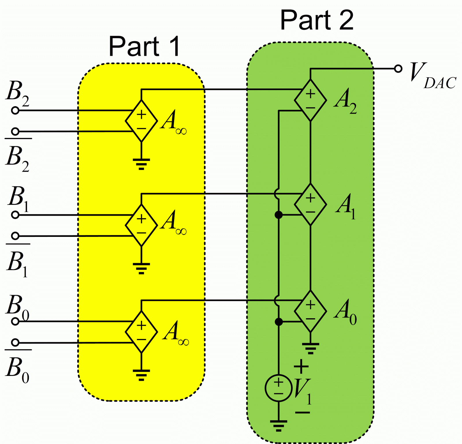
Figure 1: An example 2 bit ideal DAC
Now, we will examine the ideal DAC in details. In the left side we have differential output bits of the example two bit A/D. If you have a single-ended circuit you can simply change the Bi! (NOT of Bi bit) pins with a Vdd/2 voltage.
Part one (the yellow rectangular) rounds the output bits of the main A/D. This can be done by adjusting three parameters of the related VCVSs. The first parameter is voltage gain of these VCVSs, which should be selected to a very high quantity (e.g. 1000). On the second place, we are to choose a Max and Min for the output voltage. It is rational to choose them symmetrically around zero to have a bipolar code but the minimum cannot be less than zero in a VCVS! Consequently, we are forced to choose a non-negative quantity for Min. We can choose any pair of voltages for Max and Min and then compensate it in part 2 (I suggest +2 v and 0 v for Max and Min, respectively). Briefly, we choose voltage gain, Max and Min of the VCVSs of the first part as:
Av=1000; Max=+2 v; Min=0 v.
This arrangement provides a code with +2 v and 0 v output voltages.
Part two does two acts:
- It shifts the output code voltages from [+2 v, 0 v] to [+1 v, -1 v] by subtracting 1 v voltage from first part outputs.
- It combines the bits to provide the final DAC voltage.
In this part, no Max or Min is selected for the VCVSs. The gain for each VCVS (Ai) is selected by the output bits type. If it is thermometer code you must adjust all gains similarly (A0=A1=...=1) but if the output code is binary, you must adjust gains exponentially (i.e. A0=1, A1=2, A2=4, A3=8, . . .). The VDAC is now the targeted DAC voltage.
NOTE1: The output of this DAC is valid only at the time which all Bi's are valid.
NOTE2: This DAC is not applicable in pipelined A/D and also MASH sigma-delta modulators. Some changes are necessary and I'll explain them in another post.
NOTE3: The absolute quantity of the all parameters are not important in the FFT results, for example for a binary code you can choose the following gains: (i.e. A0=0.5, A1=0.25, A2=0.125, A3=0.0625, . . .). Also, in the first part you may choose [+10 v, 0 v] for Max and Min and 5 v for V1 voltage source.
thanks very much
ReplyDeleteIt's very helpful. Thank you!
ReplyDelete